VIEW ONLINE: > Article source
MEMS is a complex, interdisciplinary industry with a wide diversity of devices, processes and no defined production roadmap. Indeed, the Yole MEMS law “One MEMS, One process” still rules the MEMS production. But the MEMS & sensors industry is facing new challenges today such as cost & size reduction, reduced time-to-market, new sensing functionalities. These challenges are mostly driven by the consumer and portable / wearable electronics applications…
Solutions to overcome these challenges are existing such as optimizing MEMS processes or developing breakthrough approaches. You can learn more about these challenges and solutions in the recent report from Yole Développement and OMNT on New Detection Principles & Technical Evolution for NEMS & MEMS (more information here). This last approach is the one Tronics Microsystems (Tronics) decided to adopt. Indeed, as the MEMS industry is looking for new sensing principles for smaller, more functionalized devices, M&NEMS from Tronics is very promising. We have the pleasure to interview Stéphane Renard, founder and CTO of Tronics about M&NEMS status at Tronics, and we are pleased to share it with you!
Yole Développement: Could you make a short introduction on Tronics and its activities?
Stéphane Renard: Tronics is an international full-service MEMS manufacturer with wafer fabs in Europe and the USA, and representation in Asia. We offer one of the broadest technology portfolios in the industry and our services range from MEMS design to high volume MEMS manufacturing.
Tronics is “much more than a MEMS foundry” in the sense that we offer the full service spectrum of competencies required for successful transformation of OEM concepts into reliable MEMS products, including comprehensive test and packaging capabilities.
YD: What are at the moment the news on Tronics and how is 2014 going for you?
SR: Tronics offers comprehensive engineering, manufacturing and technology solutions for the MEMS market.
MEMS Manufacturing and Design Services
This activity, which was and remains today the main part of the company business, provides custom MEMS products to industrial partners (including design, packaging and test services when necessary). The customers for these services are spread all over the world and are active in a large variety of activities, such as industrial, medical or aerospace applications.
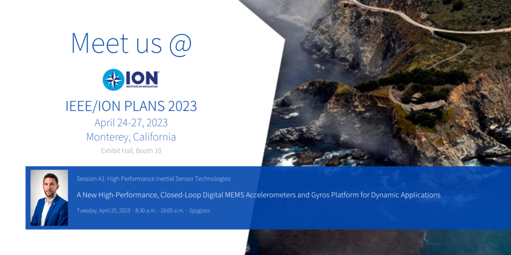
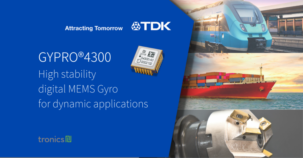
High Performance Inertial Products
TRONICS is the only independent European supplier of both high performance MEMS Accelerometers and Gyros. The GYPRO product line is made of sub-1°/h MEMS gyros targeting applications that are more demanding than automotive, while not requiring ‘tactical grade’ FOG or DTG. AXO product line is a development of MEMS accelerometers enabling a new level of performance thanks to its closed-loop architecture. All products are manufactured in our wafer fab, assembly and calibration lines located in France.
Technologies for Consumers Markets
Tronics offers two technology platforms for the manufacturing of ultra-miniature multi-DOF MEMS sensors. One is M&NEMS technology; the other one, called MAGELAN, provides miniature capacitive MEMS structures, which can be designed into accelerometers, gyroscopes and more generally a wide range of comb-driven structures.
YD: Can you tell us more on the status of the M&NEMS technology at Tronics ?
SR: After industrializing the CEA-Leti’s M&NEMS technology, Tronics has developed a new generic technology platform for integrated multiDOF sensors based on this breakthrough piezoresistive nanowires detection principle.
Building on our experience in high performance capacitive MEMS technologies, and our know-how in DRIE, wafer bonding and Vacuum Wafer Level Packaging, we have designed a manufacturable process flow that combines traditional inertial MEMS blocks and sub-micronic processing technology. This process flow is currently being patented.
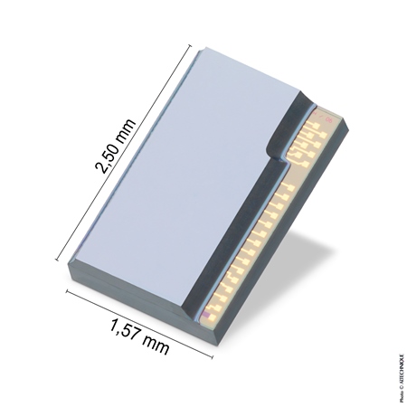
Early 2014, a single-chip 6 DOF MEMS (3 accels + 3 gyros), smaller than 4 mm², has been manufactured. In parallel, a single-chip 9DOF demonstrator has been designed.![]()
The principle of a single-chip 10DOF sensor, including a pressure sensor, is now under investigation.
YD: What are the key differentiators of this technology compared to the comb drive structure?
SR: The first key differentiator is the size reduction. By using tiny piezo-resistive silicon nanowires instead of surface-consuming capacitive comb electrodes for signal transducing, each active part of the sensors can be significantly reduced. In this way, we have been able to design a 6DOF sensor, as small as 4 mm², with totally separate structures for each sensing axis. Further design iterations will enable more drastic size reductions.
Besides its size advantage, the technology significantly decreases power consumption, more specifically for high-frequency magnetometer, and enables the manufacturing of accelerometers, gyroscopes, magnetometers and pressure sensors using the same process flow.
Moreover, the piezo-resistive detection is simplifying the electronic interface, reducing the ASIC size and, at the end of the day, shrinking the component footprint.
YD: The smallest MEMS accelerometer today is the Bosch BMA355 (3 axis accelerometer). Will M&NEMS allow smaller dies?
SR: M&NEMS technology has a huge advantage in terms of size reduction. We are not currently manufacturing stand-alone 3axis accelerometer, but, with some design optimization, smaller dimensions are achievable.
YD: What is the other products roadmap for M&NEMS technology?
SR: Presently, a single-chip 6DOF MEMS IMU (3 accelerometers + 3 gyros) is in manufacturing. Technology upgrades are on-going and a single-chip 9DOF demonstrator is being processed. Next design on the roadmap is a single-chip 10DOF integrating a pressure sensor. In parallel, TRONICS starts to design the 2nd generation of inertial combo MEMS.
The M&NEMS technology is a generic platform that enables the manufacturing of a wide variety of combo sensors just by changes in the design. Those combo sensors can combine accelerometers, gyroscopes, magnetometers, and soon pressure sensors or microphones.
YD: As this technology is very new, what are the challenges for materials / equipment manufacturers to supply the right tool? Or is M&NEMS using “standard” MEMS tools? What are the key manufacturing challenges (lithography, etching, data processing …)?
SR: This is an important point: the M&NEMS technology is using standard MEMS tools that you can find in any volume MEMS foundry.
As an example, for the lithography, the minimum critical dimension is 0.5 µm, which is today quite common with well-established i-line stepper.
YD: How do you see the next steps for the introduction of the M&NEMS technology on the market?
SR: With the delivery of miniature 6DOF MEMS IMU chip, the main technical challenges linked to the manufacturing of the nanowires have been successfully addressed. Manufacturing of this product is on-going. Furthermore a 9DOF and other combo sensors are being developed. The final products will be commercialized by our partners.
YD: Can you comment on the business model shift from a MEMS foundry specialized in high end applications to a MEMS player targeting consumer applications?
SR: This new M&NEMS technology, which constitutes a real breakthrough for combo sensors, is completing a growing portfolio of submicronic technologies at Tronics. Using nano-imprint lithography or other submicronic processes, Tronics is already manufacturing high performance optical mirrors and optical components. We believe that today, innovation is coming from the consumer market. A MEMS foundry, whatever its target markets are, must have in its portfolio the most advanced consumer technologies and designs.
This is what Tronics has achieved with the M&NEMS platform.
YD: How will Tronics be prepared to cope with increasing market volume?
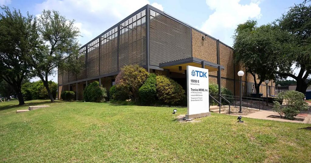
SR: Tronics has 6-inch wafer fabs in both Grenoble and Dallas. The first is capable of 10k wafers per year and the second 50k wafers per year. And for huge-volume consumer MEMS production, Tronics can outsource production to a 200mm wafer fab in Asia.
YD: Do you see any competing technologies able to replace the comb drive structure in inertial sensing?
SR: We know that some other approaches, such as resonating BAW mechanics, are under investigation to compete with the mainstream comb drive structures, and also the M&NEMS technology. But we think that M&NEMS is the most advanced technology and the only one that enables single-chip integration of such a variety of different sensors; with such a small foot print, low power consumption and simplified electronic interface.
Stephane RENARD is the founder and CTO of TRONIC’S Microsystems.
He received his engineering degree from Ecole Centrale de Paris (1979) and his PhD degree from Grenoble-INP, the Grenoble Institute of Technology (1983). In 1983, he joined LETI (CEA) where he participated in various R&D projects and technology transfers in optoelectronics.
From 1991 to 1997, he managed LETI’s micro-sensors and MEMS R&D team; the one that invented the in-plane MEMS capacitive accelerometer and the MEMS on SOI technology.
In May 1997, Stephane Renard founded Tronic’s Microsystems: the first private European company specialised in the manufacturing of dedicated SOI MEMS. The company grew steadily in the last 15 years, and has been profitable since 2006. With wafer fabs in Europe and the USA, Tronics is now, one of the largest independent full-service MEMS manufacturers.
Source: Yole Développement and Tronics Microsystems